TMS 9995 Breadboard or PCB System
Page Contents
 Description
 Specification
 Parts List
 Technical Description
 References
 Assembly
 EPROM Binary Images
 Switching On, Testing and Fault-Finding
 Programming - System Monitor
 Programming - BASIC
 Programming - Forth
 Expansion and Future Development Ideas
 Building on the PCB
Description
This simple TMS 9995 system is aimed at users with little or no hardware skills who want to build their own functional microcomputer. The system can be built either on a breadboard, or on a PCB which can be purchased from me.
The project is based around the Texas Instruments TMS 9995 16-bit microprocessor and guides the user through building a fairly minimal system using readily available components. If building on the breadboard, no soldering or circuit layout skills are required with the exception of soldering a couple of wires onto a connector.
The microcomputer is designed to interface with a Terminal program running on a PC, and run a system monitor, BASIC interpreter and Forth interpreter from EPROM - note though that there is no facility to load or save programs on this simple system
except by downloading or uploading them over the serial interface. Preprogrammed EPROMs are available for purchase for users who do not have the facilities to program their own.
The breadboard system is easy to modify, expand and experiment with as the user wishes. The PCB includes provision for an expansion connector to enable the system to be expanded off the board.
Most of this web page relates to building the project on a breadboard. Building on the PCB requires the same components (plus another resistor and an LED) and uses the same EPROM images; further details are included here.


Specification
- 16-bit TMS 9995 microprocessor running at 3 MHz (12 MHz clock internally divided by 4).
- 32K byte 27256 or 27C256 EPROM.
- 32K byte 62256 static RAM.
- RS-232 serial port with Baud rate autodetected (300 Baud to 19200 Baud).
- Single +5V @ 200mA power supply requirement.
- Reset switch.
Parts List
The project requires the parts listed in the table below. Approximate (UK) costs are included.
You should be able to get everything off eBay if you don't want to use a
specialist supplier such as Digi-Key.
Capacitor voltages can be the specified value or greater.
All resistors are 0.25W - 0.6W, 6mm body length.
| - |
2 pieces of solderless breadboard, each section approx. 175 × 65 mm (64 contact points (holes) long by 10 wide, 2 pairs of bus strips along each edge of the board, see this photo) |
£7 for the 2 sections |
| U1 |
TMS 9995 microprocessor |
£10 - £30 (ignore the overpriced ones on eBay at £140!) |
| U2 |
32K byte 27256 or 27C256 EPROM, 300ns or faster (ST part # M27256-2F1 and M27C256B-70XF1 work) |
£7 for 10 - should be obtainable singly if needed |
| U3 |
32K byte 62256 static RAM, 300ns or faster (Cypress Semiconductors part # CY62256LL-70PXC works) |
£1 |
| U4 |
74LS04 hex inverter IC |
£1 |
| U5 |
74LS32 quad 2 input OR gate IC |
£1 |
| U6 |
MAX232CPE+ dual RS-232 transceiver |
£1.50 |
| U7 |
TMS 9902ANL asynchronous communications controller |
£10 (ignore the overpriced ones on Ebay at £140!) |
| U8 |
74LS138 3-to-8 line decoder IC |
£1 |
| X1 |
12 MHz crystal, HC-49U package (AEL Crystals part # X12M000000L188 or Fox Electronics part # FOXLF120 works) |
£2.50 |
| C1, C2 |
15pF ceramic capacitor |
£0.35 for the 2 |
| C3 - C9 |
0.1μF ceramic decoupling capacitor |
£2.50 for the 7 |
| C10 - C14 |
1μF electrolytic capacitor, 16V |
£1.75 for the 5 |
| C15 |
22μF electrolytic capacitor, 16V |
£0.30 |
| C16 |
0.01μF (10nF) ceramic capacitor |
£0.40 |
| R1 - R5 |
1K metal film 0.6W resistor |
£1.20 for the 5 |
| R6 |
10K metal film 0.6W resistor |
£0.30 |
| SW1 |
Single pole, push-to-make, PCB mount, non locking switch |
£1.20 |
| J1 |
9-way D-type socket (female), solder terminals |
£2 |
| - |
Wire for connections on breadboard. Either use packs of jump leads specifically designed for breadboards, or use 0.6mm solid core wire cut to length and ends stripped. Preferably get 5 different colours to use for power, ground, address bus, data bus and control signal connections. |
- |
| - |
+5V 1A regulated power supply. Alternatively, get a USB power cable with a barrel DC power connector and power the board from the PC that you're no doubt sitting next to. |
- |
| - |
Suitable connector to connect power supply to breadboard |
- |
Optional - ZIF socket adaptor recommended if changing the EPROM frequently: |
| - |
28 pin ZIF socket |
£3 |
| - |
0.1 inch pin strip (solder to ZIF socket to form pins to insert into breadboard) |
£1.30 |
Optional - EPROM eraser and programmer if you want to program your own EPROMs: |
| - |
EPROM eraser |
£4 upwards |
| - |
EPROM programmer |
£25 upwards |
Useful for fault-finding: |
| - |
Digital multimeter |
£5 |
| - |
Logic probe |
£15 |
Technical Description
A circuit diagram for the project is available here. The following description should be read in conjunction with the component datasheets, links to which are given in the References section below.
Processor U1 derives its clock from 12 MHz crystal X1. The crystal frequency is internally divided by 4 to give a processor clock speed of 3 MHz.
No processor interrupts are used in the system, so the processor /INT1, /INT4_/EC, and /NMI inputs are tied high by resistors R1, R2 and R3.
Direct memory access (DMA) by external devices is not used in the system so the processor /HOLD input is tied high by resistor R4.
The processor /RESET input is normally pulled high by resistor R6. To reset the processor, switch SW1 is pushed to pull the /RESET input low. Capacitor C16 debounces the switch contacts. Note that a 'power-on reset' function is not implemented.
EPROM U2 and static RAM U3 are connected to the processor address and data buses. Note that at the time Texas Instruments labelled their address and data bus lines the opposite way round to the rest of the industry, so the low numbered processor address and data bus lines are connected to the high numbered EPROM and RAM address and data bus lines, and the high numbered processor lines are connected to the low numbered EPROM and RAM lines. The EPROM and RAM /OE (Output Enable) inputs are connected to the processor /DBIN output, which when active low indicates that the processor has disabled its data bus output buffers to allow external memory to output data onto the data bus. The EPROM /CE (Chip Enable) input is derived by ORing address bus line A0 with the processor /MEMEN (Memory Enable) output, such that the EPROM is enabled during memory cycles in the address range >0000 - >7FFF. The RAM /CE input is derived in a similar way by inverting address bus line A0 and ORing it with /MEMEN such that RAM is enabled during memory cycles in the address range >8000 - >FFFF.
3-to-8 line decoder U8 decodes address bus lines A7, A8 and A9 during CRU input/output cycles when /MEMEN is high to provide chip enable signals for 8 blocks of 32 bits of CRU address space. Output /Y0 is active low when addressing CRU bits 0 - 31, /Y1 is active when addressing bits 32 - 63, and so on.
TMS 9902 Asynchronous Communications Controller (ACC) U7 is a CRU peripheral device which provides the interface between the processor and a serial, asynchronous, RS-232 communications channel. The connection to address decoder U7 maps the device to processor CRU address bits 0 - 31. RS-232 driver/receiver U6 generates ±10V supplies from the single +5V supply and provides signal level conversion between RS-232 signal levels (±3V to ±25V) and the TTL signal levels used by U7. A simple 3-wire RS-232 interface is implemented through connector J1.
Capacitor C15 provides power supply smoothing. The supply to individual ICs is decoupled by capacitors C3 - C9.
Wait States
The processor READY input is tied high by resistor R5 to enable the processor 'automatic first wait state generation' feature when it is reset. This can be inhibited if desired as detailed in the TMS 9995 data manual (it is controlled by the state of the processor READY input when the /RESET input is released). The access times specified for the EPROM and RAM are sufficient for the processor to run with a single wait state for each external memory cycle, and may work with no wait states - you'll have to experiment!
Note that the system monitor software that can be downloaded from this web page autodetects the terminal Baud rate by means of a timing loop that measures the length of the start bit of a character transmitted over the RS-232 interface. Changing the number of memory wait states and/or changing the processor clock speed will require recalculation of the timing loop counts and a new EPROM being programmed. Alternatively, the software could be tweaked to always use the same Baud rate.
Can't /RAM_CE Simply be 'NOT' /ROM_CE?
Someone asked me why the /RAM_CE signal cannot simply be generated from an inverted /ROM_CE signal. If the processor isn’t accessing ROM then it must be accessing RAM, right? Wrong! The truth table below shows the state of the /ROM_CE and /RAM_CE signals for each combination of /MEMEN and A0. Remember that /MEMEN is low during a memory access and high at all other times such as during a CRU (I/O) access. ROM and RAM are enabled (reading data or writing data to the data bus) when their respective /CE input is low. So it can be seen that ROM is enabled during a memory access when A0 is low, and RAM is enabled during a memory access when A0 is high. Both ROM and RAM are not enabled when a memory access is not occurring (/MEMEN is high). The last column in the table shows the inverted /ROM_CE signal; if this was used to enable the RAM, then RAM would be enabled when /MEMEN is low and A0 is high, which is what we want, but RAM would also be enabled when memory accesses are not occurring, which in some systems could potentially lead to some interesting RAM corruption during CRU cycles as the memory /WE signal shares the same processor pin as the CRU clock /CRUCLK signal ...
| 0 |
0 |
0 |
1 |
1 |
| 0 |
1 |
1 |
0 |
0 |
| 1 |
0 |
1 |
1 |
0 |
| 1 |
1 |
1 |
1 |
0 |
References
TMS 9995 processor data manual
ST M27256 EPROM data sheet
Cypress Semiconductors CY62256 static RAM data sheet
74LS04 hex inverter IC data sheet
74LS32 quad 2 input OR gate IC data sheet
MAX232CPE dual RS-232 transceiver data sheet
TMS 9902ANL asynchronous communications controller data sheet
74LS138 3-to-8 line decoder IC data sheet
System monitor. The project uses the EVMBUG system monitor from TI's
TMS 9995 Evaluation Module.
EVMBUG is described on this page.
The BASIC interpreter is based on a port of the Powertran Cortex Power BASIC made for my TM 990 computer. The Cortex BASIC user guide is available here.
The Forth interpreter is based on fig-FORTH 9900 Release 1.0 (March 1981). Details on fig-FORTH are available at www.forth.org.
Assembly
Assembly is fairly straightforward as long as a methodical approach is taken. Although there are quite a few connections to make, making each individual connection is relatively easy. It is a good idea to print off the circuit diagram so you can see the signal pin numbers and to mark each connection as you make it.
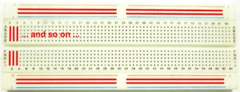
Before starting, it is necessary to understand how the contact points on the breadboard are electrically connected together within the board. Looking at the picture below, the contact points along each of the lines are connected (but those along one line are not connected to those on another). Along each edge of the board is a pair of bus strips, with one strip of each pair for +5V, and the other for Ground. Note how each pair of bus strips is split into two, and requires jumper wires to connect the buses along the length of the board. As the board layout can vary between designs and manufacturers, use a multimeter and a pair of jumper wires to verify the continuity between the groups of contact points.

Start by joining together the two sections of breadboard along their long edges. Most have lugs along their edges that enable them to be fixed together. Then add jumpers to connect the two halves of each row of bus strips together, and to connect each of the +5V bus strips together and the Ground bus strips together across the two sections of board.
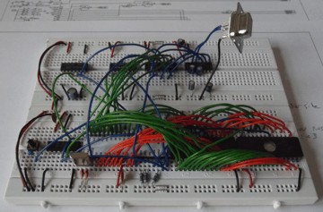
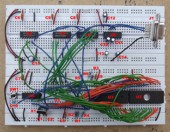
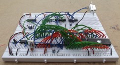
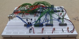
Next, position the ICs. The first photo below (click image for a larger view) shows the component layout I have used. The exact positions of the ICs is not critical - although I would advise that the EPROM is at the end as it makes it easy to remove and replace with a newly programmed EPROM. The second and third photos below (click for a larger view) show front and rear views of the project. All the ICs are oriented with the notch pointing to the left, so in the first photo pin 1 on each IC is at the bottom left of the chip.


A label showing the pinout of the TMS 9995 processor can be downloaded here, printed and lightly stuck to the top of the processor IC to aid making connections to the right pins.
Next, connect the power supply pins of each IC to the nearest power supply bus strips and add the power supply decoupling capacitors. Follow this with the resistors which can lay flat on the board, the crystal and its capacitors, and the reset switch and its capacitor.
The final task is to add the connections between the ICs. The following notes may be helpful:
- I suggest you use one colour of jumper/wire for the address bus connections, a second colour for the data bus, and a third colour for the remaining control and clock signals, as shown in the photo; this will make it easier to trace any problems later.
- Note how the connections that are going to both the RAM and EPROM are made first from the processor to the RAM, and then from the RAM to the EPROM.
- Although most of the signals on the RAM and EPROM are on the same pins on each IC, there are some exceptions. Check the pin numbers of each IC on the circuit diagram carefully. Note also that some of the address bus pins jump around; they are not on consecutively-numbered pins.
- After making a few connections, it might be worth using the multimeter on low resistance range to check the connections by testing for continuity between the appropriate IC pins. This will force you to check the circuit diagram again and find the correct pins on the ICs themselves; it is easier to find and correct any mistakes now rather than later. Then make a few more connections and check those, and so on.
- Try not to route any connections directly over the top of the EPROM as this makes it easier to remove and replace with a newly programmed EPROM.
- If you later want to use a ZIF socket for the EPROM, leave a clear set of holes along each side of the EPROM as shown in the photo to give enough space for the socket.
EPROM Binary Images
Link to EVMBUG system monitor EPROM image here.
Link to EVMBUG system monitor and BASIC EPROM image here (BASIC
runs from RAM).
Link to EVMBUG system monitor and BASIC EPROM image here (BASIC runs from EPROM).
Link to EVMBUG system monitor and Forth EPROM image here.
Link to test EPROM image #1 here - see Testing and Fault-Finding section below.
Link to test EPROM image #2 here - see Testing and Fault-Finding section below.
Link to test EPROM image #3
here - see Testing and Fault-Finding section below.
The 27256 or 27C256 EPROM used is fairly common and most modern EPROM programmers will be able to program it. If you can't program it yourself and can't find anyone else to do it for you, drop me an e-mail (ti99@stuartconner.me.uk) and we'll work something out. Note that I live in the UK, so postage to the US for example will cost a few dollars.
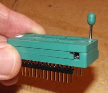
If you want to swap EPROMs frequently, consider making a ZIF socket adapter to plug into the breadboard - see the photo below. The adaptor simply comprises a 0.1 inch pin strip soldered directly to the ZIF socket to form a rigid set of pins that will plug into the breadboard.

Switching On, Testing and Fault-Finding
Give the components and wiring a final check, then connect the +5V power supply using a pair of wires to any of the power supply bus strips. Switch the power supply on, and using the multimeter check for +5V across U4 pins 7 and 14, and U2 (the EPROM) pins 14 and 28 (these should be fairly easy to get to with the multimeter probes). If all is OK, check for +10V across U6 pins 15 and 2, and for -10V across U6 pins 15 and 6, and then switch power off. If any power supply problems are found, check your wiring.
Next, connect D-type connector J1 to the PC using a standard RS-232 serial cable, being careful not to dislodge the connector wires where they are pushed into the breadboard (I've had the project running OK using a USB serial port adaptor). Start a Terminal program on the PC (Tera Term Pro is a good program - Google for it) and configure the serial port on the PC for 7 bits/character, even parity, 2 stop bits, no flow control (handshaking). The system will work with the following Baud rates: 300, 600, 1200, 2400, 4800, 9600, 19200, so configure the port to one of these.
Switch power back on, press and release the reset switch SW1, then type 'A' (uppercase A) or <Return> and the system will autodetect the Baud rate and reply with the message "EVMBUG R1.0" followed by the command prompt "MON?".
If the system is not working, follow these fault-finding steps:
- Check that the serial port is correctly connected and configured on the PC, as described above.
- Using a logic probe, check for activity on U7 pin 3 when a key is pressed on the PC (with the Terminal program running and active). This is where the serial data from the PC is input. If there is no activity, this indicates a problem with U6, the connection to J1, the connection to the PC, or the configuration of the serial port on the PC.
- Using a logic probe, check for activity on U7 pin 2 when a key is pressed on the PC. This is where serial data is output to the PC. If a signal is seen here but there is no response on the PC, this again indicates a problem with U6, J1, or the connection or configuration of the serial port on the PC.
- Using a logic probe, check for a continuous clock signal on U7 pin 16. This is the clock output from the processor, and indicates that the processor clock is running.
- Using a logic probe, check that U1 pin 22 is high, and goes low when the reset switch is pressed. This is the reset input to the processor.
- There are three test EPROM images (download links above) that can be used
to test the basic functionality of the system:
- The first test image tests just the processor, the EPROM and the EPROM chip select logic. Program and fit the EPROM, power on, press the reset switch, then use the logic probe to check for a series of pulses on U2 pin 20 every 2 seconds or so. If no activity is seen, consider removing all the connections between the ICs except those between U1, U2 and U5 and try again, in case one of the connections is wrong and is interfering with the correct operation of the processor buses.
- If the first test passes, repeat with the second test image, which also tests the RAM and the RAM chip select logic. With the second test, a series of pulses should be seen on U2 pin 20 every 6 seconds or so. If the first test passes but the second fails, check for activity on the RAM chip select input U3 pin 20; if no activity is seen, check the wiring to U3, U4 and U5.
- The third test image configures the serial port to
9600 Baud, 7 bits/character, even parity, 2 stops bits, no flow control,
and then loops continually sending the ASCII characters >21 ("!") to >7E
("~"). This tests most of the system including transmitting through the
serial port. If the previous two tests pass but this test fails, check the
connections to U8, U7 and U6 (and also ensure that the serial port on the
PC is configured correctly). It will be necessary to press the reset
switch after applying power for this test to start.
- If all the tests and checks have passed so far, then the system should be working. Drop me an e-mail (ti99@stuartconner.me.uk) and I'll see if I can help you further.
Programming - System Monitor
The project uses the EVMBUG system monitor from TI's TMS 9995 Evaluation Module to provide an interactive interface between the user and the system.
EVMBUG is described on
this page.
If you are new to programming a single board computer of this type, the user manual for the TM 990/100M microcomputer (which is based on the earlier TMS 9900 processor) provides a good introduction to the processor architecture and concepts.
The tag format loader LMC command can be used to download a program assembled using the Asm99/4a assembler on the PC. A utility is required on the PC to feed the program object code to the serial port - details TBD.
Programming - BASIC
The BASIC interpreter is based on a port of the Powertran Cortex Power BASIC made for my TM 990 computer. BASIC is programmed in the EPROM along with a slightly modified version of the EVMBUG monitor.
Two versions of BASIC are available (in different EPROM images):
- In one version, the BASIC interpreter code is copied from the EPROM into
RAM and then run from RAM. This leaves 3K of memory free for program storage
- but this is often sufficient for 'tinkering', and it is possible to tweak
the BASIC interpreter itself if required as it is resident in RAM.
- In the second version, the BASIC interpreter code mostly runs direct
from EPROM. This leaves 22K of memory free for program storage.
When the system is reset and the Baud rate detected, a menu is displayed: press 1 to run the EVMBUG monitor, or press 2 to run BASIC.
TMS 9995 BREADBOARD SYSTEM
BY STUART CONNER
PRESS 1 FOR EVMBUG MONITOR
PRESS 2 FOR CORTEX BASIC
(Press 2)
-- TMS 9995 BREADBOARD BASIC Rev. 1.1 --
[Ported from Cortex BASIC (C)1982 by Stuart Conner]
*Ready
The Cortex BASIC user guide is available here.
Mapping between the keys on the Cortex computer and the keys on the PC keyboard is as shown in the following table.
| Enter |
Return |
| Edit |
Ctrl-T |
| Clear |
Ctrl-L |
| Escape |
Esc |
| Graphic |
(not supported) |
| Insert |
Ctrl-V |
| Delete |
Ctrl-C |
| Rubout |
Backspace |
| Cursor Up |
Ctrl-E |
| Cursor Down |
Ctrl-X |
| Cursor Left |
Ctrl-S |
| Cursor Right |
Ctrl-D |
| Home |
Ctrl-H |
The version of EVMBUG supplied with BASIC is modified such that the automatic delay functionality after printing each line on a mechanical teletype is disabled. This won't make any difference unless you happen to be using a mechanical teletype ...
When BASIC is in use, all input is automatically converted to upper case.
There are some changes and restrictions in the TMS 9995 breadboard implementation as compared to the implementation described in the Cortex user guide:
- The following commands are not supported, and will display an error message if used: BOOT, MON, TIC, BAUD, MOTOR, TIME, LOAD, SAVE.
- The commands associated with text and graphics displays will be accepted and will execute, but as the system does not include a display processor, nothing will be seen.
- Extended commands *LOAD, *SAVE, *DIR and *DELETE will be recognised but are not functional (they will crash the system).
- The UNIT command supports a value of 2 only (all input and output over the RS-232 interface).
- Pressing the <Space> key pauses a listing, then pressing any key resumes the listing. Stepping through the listing line-by-line is not currently supported.
- SYS values 10, 13-17, 19 are not relevant and will return -1.
- A new SYS value of 20 returns the address of the colour substitution table used by the SWAP command (see the addendum to the COLOUR command on page 4-77 of the user guide).
- The WAIT statement without an argument returns immediately. With an argument, no input is accepted and the <Escape> key is not active until the wait period expires. The wait period is significantly shorter than the 0.01 seconds quoted.
- There is a bug in the original implementation of the CHAR statement. When typing in a program, you need to put a space between the line number and the CHAR statement otherwise an 'Illegal Character' error is displayed.
- Memory addresses mentioned in the user guide and the memory maps are not correct for the TMS 9995 breadboard implementation. I can provide memory usage details if required.
Programming - Forth
The Forth interpreter is based on the fig-FORTH 9900 Release 1.0 (March 1981). The source code is available here (the TMS 9995 breadboard implementation is slightly modified in terms of the memory pointers used and the input/output routines). Forth is programmed in the EPROM along with a slightly modified version of the EVMBUG monitor. When the system is reset and the Baud rate detected, a menu is displayed: press 1 to run the EVMBUG monitor, or press 2 to run Forth.
TMS 9995 BREADBOARD SYSTEM
BY STUART CONNER
PRESS 1 FOR EVMBUG MONITOR
PRESS 2 FOR FIG-FORTH
(Press 2)
9900 fig-FORTH Rel 1.0
The Forth code is copied from EPROM to RAM and then run from RAM when it is selected at the menu. All input and output is over the RS-232 interface, and there is no means of loading or saving a program.
Various Forth tutorials are available here. Note that different versions of Forth support slightly different dictionaries so you might find some examples in the tutorials that will not work on the TMS 9995 breadboard implementation.
The version of EVMBUG supplied with Forth is modified such that the automatic delay functionality after printing each line on a mechanical teletype is disabled. This won't make any difference unless you happen to be using a mechanical teletype ...
Expansion and Future Development Ideas
Now you have a basic working system, expansion is fairly easy, up to the point where the system has so many wires that you keep on knocking them out of place! At that point of course you might want to consider assembling the basic system more permanently on a piece of stripboard, and connect that to the breadboard where you can experiment with further components.
The following paragraphs provide some future development ideas. Software to use with them can be written and assembled on the PC using the Asm99/4A assembler and downloaded to the system using the tag format loader LMC command in EVMBUG. A utility is required on the PC to feed the program object code to the serial port - contact me for details.
The CRU address space is already being decoded by U8 so adding another CRU peripheral IC is fairly easy - wire it up in the way as TMS 9902 U7 and use a different chip select output from U8. If you wanted to add a second TMS 9902 for another RS-232 port, there are spare connections in U6 for signal level conversion. Adding a TMS 9901 (data sheet here) would enable you to drive LEDs and read switch positions; inputing data from a keyboard with a parallel ASCII output is also a possibility.
Memory can be organised in a more flexible way by decoding address lines A0 - A3 using a 74LS154 4-to-16 way decoder, using /MEMEN as one of the /G enable inputs. This gives 16 active low chip select signals, the first of which is active when a memory address in the 4K memory block >0000 - >0FFF is accessed, the second for 4K memory block >1000 - >1FFF, and so on. Different combinations of chip select signals can be used to map EPROM and RAM to different areas in the memory address space. The circuit diagram here shows the use of a 74LS154 in a TMS 9900 system to enable RAM in selected memory blocks and to write-protect selected blocks.
Memory blocks do not have to be populated with memory; they can be used with 'memory mapped devices' that appear to the processor as memory but which provide input/output functionality. This technique is illustrated in the circuit diagram here where a 74LS138 3-to-8 line decoder divides the memory address space into eight 8K blocks, then one of these blocks (selected by a jumper) is divided by a second 74LS138 into separate 1K blocks within the 8K block. One of the outputs from the second 74LS138 is used as a chip select for a peripheral device. Dividing the memory address space down to a 1K block allows many devices to be slotted into the memory address space with minimal loss of room for RAM and ROM. Sheet 2 of the circuit shows an interface for a 6581 SID device - the sound generator chip used in the Commodore 64 computer. The data bus and the least-significant 5 bits of the address bus are latched when a write is made to device's mapped address space and output continually to the SID device. Sheet 3 of the circuit shows an interface for a TMS 9918A video display processor (data sheet here). Logic gates (on sheet 1) generate the separate read and write chip select signals required by the device, which are only active in the device's mapped address space.
Enjoy!
Building on the PCB

(Click image for larger view) |
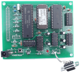
I have available a PCB for this project, laid out by Michael C in Australia to my circuit diagram (Michael's website is here, and he has a few PCBs and other bits available as well if you live in that part of the world). The PCB uses the same components as the breadboard system described above, and uses the same component markings/IDs. Two additional components are required for the power LED fitted to the board: R7 is a 220 Ohm resistor, and the unmarked LED is just a standard 3mm or 5mm LED. (When fitting the LED, the longer lead goes on the side of the 'flat' on the component marking.)
The PCB also includes an (optional) expansion connector (J2). This has the same pinout as the TMS 9995 itself, with the exception of the oscillator pins. The connector does not have to be fitted, and is provided merely as a convenience should you want to tinker with the hardware yourself. Connector J3 is designed for jumper pins to connect/disconnect the pullup resistors for some of the unused processor control signals. Each pullup resistor can be disconnected if the signal is to be driven through the expansion connector. If not using the expansion connector, these jumper pins can be replaced with simple wire links.
The RS-232 port connector (J1) is laid out for a rectangular connector, not the usual D-type connector. If you want to use a D-type connector, you will have to do a little bit of hard-wiring to it (connect pins 2, 3 and 5 on J1 to pins 2, 3 and 5 on the D-type connector).
The type of power connector fitted is up to you, depending on how you intend to power the board. |

 Description
 Specification
 Parts List
 Technical Description
 References
 Assembly
 EPROM Binary Images
 Switching On, Testing and Fault-Finding
 Programming - System Monitor
 Programming - BASIC
 Programming - Forth
 Expansion and Future Development Ideas
 Building on the PCB