TMS 9900 Breadboard or PCB System
Page Contents
 Description
 Specification
 Parts List
 Technical Description
 References
 EPROM Binary Images
 Assembling the PCB
 Connecting to the Serial Port
 Versions of Cortex BASIC
 Programming - TIBUG and EVMBUG System Monitors
 Programming - BASIC
 Programming - Forth
 Examples of Using the EVMBUG IC (Inspect/Change CRU) Command
 CRU Instruction Displacement Counts
 Project - TMS 9901 to IDE Interface
 Project - SBP 9900/9989
Processor Adaptor Board
Description
This TMS 9900 system project provides a similar, minimal system to my TMS 9995 breadboard project, but using the Texas Instruments
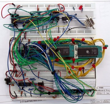
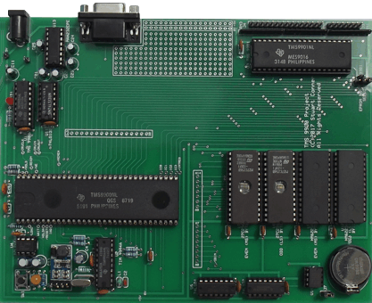
first-generation TMS 9900 16-bit microprocessor. The system can be built either on a breadboard, or on a PCB (contact me if you want a PCB - I'll order them in small batches once a couple of people have expressed an interest).
The microcomputer is designed to interface with a Terminal program running on a PC, and run a system monitor, BASIC interpreter and Forth interpreter from EPROM - note though that there is no facility to load or save programs on this simple system
except by downloading or uploading them over the serial interface. Pre-programmed EPROMs are available for purchase for users who do not have the facilities to program their own.
The breadboard system is easy to modify, expand and experiment with as the user wishes. On the PCB, take-off points are included for all the main signals and the I/O ports to enable the system to be expanded off the board.
The PCB also includes a small prototyping area.
This web page provides the specification, circuit diagram and technical description of the system.


Specification
- 16-bit TMS 9900 microprocessor running at 3 MHz.
- TMS 9901 Programmable Systems Interface.
- 32K + 32K byte (two banks) EPROM, bank selectable through jumper or CRU output bit.
- 32K + 32K byte (two banks) battery-backed static RAM, bank selectable through CRU output bit.
- RS-232 serial port operating at 19200 Baud (7 data bits, even parity, 2 stop bits).
- Single +5V @ 300mA power supply requirement.
- Reset switch.
Parts List
The project requires the parts listed in the table below. Approximate (UK) costs are included.
You should be able to get everything off eBay if you don't want to use a
specialist supplier such as Digi-Key.
Capacitor voltages can be the specified value or greater.
All resistors are 0.25W - 0.6W, 6mm body length.
| - |
For the breadboard system, 3 pieces of solderless breadboard, each section approx. 175 × 65 mm (64 contact points (holes) long by 10 wide, 2 pairs of bus strips along each edge of the board, see
this photo) |
£10 for the 3 sections |
| - |
For the PCB version, contact me for availability of a PCB |
- |
| U1 |
TMS 9900 microprocessor |
£10 |
| U2 |
TIM 9904A clock generator |
£10 |
| U3 |
TMS 9901 programmable systems interface |
£5 |
| U4 |
ICL7660SCPAZ voltage converter |
£2 |
| U5 |
74LS32 quad 2 input OR gate IC |
£1 |
| U6 |
74LS04 hex inverter IC |
£1 |
| U7, U8 |
32K byte 27256 or 27C256 EPROM, 120ns or faster (ST part # M27C256B-12XF1 works) |
£2 each |
| U9, U10 |
32K byte 62256 static RAM, 120ns or faster, 0.6" wide package (Hitachi part # HM62256BLP-7 works) |
£5 each |
| U11 |
74LS138 3-to-8 line decoder IC |
£1 |
| U12 |
TMS 9902A asynchronous communications controller |
£10 |
| U13 |
MAX232CPE (or MAX232EPE) dual RS-232 transceiver |
£2 |
| U14 |
Dallas DS1210 non-volatile memory controller |
£10 |
| X1 |
12 MHz crystal, HC-49U package (AEL Crystals part # X12M000000L188 or Fox Electronics part # FOXLF120 works)
(Take care trying to use a crystal in a low profile HC-49/S package - I tried one of these and found the clock was unreliable, especially if you touch the capacitor and inductor forming the tank circuit.) |
£4 |
| C1 |
47μF tantalum capacitor, 16V |
£0.60 |
| C2 |
50pF ceramic capacitor |
£0.50 |
| C3, C5 - C10, C14 - C20, C26 |
0.1μF ceramic decoupling capacitor |
£1.30 for the 14 |
| C4, C11 |
22μF electrolytic capacitor, 16V |
£0.60 for the 2 |
| C12, C13 |
10μF electrolytic capacitor, 16V |
£0.60 for the 2 |
| C21 - C25 |
1μF electrolytic capacitor, 16V |
£1.75 for the 5 |
| L1 |
3.3μH inductor (choke), axial |
£1 |
| R1 - R4 |
16R metal film resistor (15R will also
work) |
£0.40 for the 4 |
| R5 |
100K metal film resistor |
£0.10 |
| R6 |
100R metal film resistor |
£0.10 |
| R7 |
4.7K metal film resistor |
£0.10 |
| R8 |
220R metal film resistor |
£0.10 |
| R9 - R11 |
10K metal film resistor |
£0.30 for the 3 |
| RN1 - RN3 |
Resistor network, 10K, 9 pin (8 commoned resistors) |
£1.00 for the 3 |
| D1 |
LED, 3mm, red |
£0.20 |
| D2 |
1N4148 diode (fitted to V2 PCB onwards) |
£0.10 |
| SW1 |
Single pole, push-to-make, PCB mount, non locking switch |
£1.50 |
| (connects to J2) |
+5V to +12V step up converter module (see eBay item number 332049746567; check pinout against PCB if using a different module) |
£2 |
| B1 |
CR2032 3V battery and PCB mount holder |
£1 |
| J1 |
DC power socket (female), 5.5 × 2.1mm, PCB mount |
£1 |
| J2 - J5, J7 |
0.1" pin strip, cut to size as required, with suitable jumpers |
£2 + £2.50 |
| J6 |
9-way D-type socket (female), PCB mount |
£2 |
| - |
IC sockets if building on the PCB (all 0.1" pin spacing):
• 1 × 64 pin, 0.9" wide
• 1 × 40 pin
• 4 × 28 pin, 0.6" wide
• 1 × 20 pin
• 1 × 18 pin
• 2 × 16 pin
• 2 × 14 pin
• 2 × 8 pin |
£10 |
Technical Description
A circuit diagram for the project is available here, and a high resolution photograph of the breadboard system
here and the PCB here. The following description should be read in conjunction with the component datasheets, links to which are given in the References section below.
TIM 9904A clock generator U2 generates the four-phase clock required by the
TMS 9900 processor U1. The frequency of the internal oscillator is established
by 12 MHz crystal X1. The LC circuit formed by inductor L1 and capacitor C2
connected across the tank inputs of U2 is tuned to the crystal fundamental
frequency. Series resistors R1 - R4 minimise overshoot and undershoot on the 12V
clock lines. The ∅3 clock, at TTL signal
levels, is also used as a timing clock for the TMS 9901 Programmable Systems
Interface (PSI) U3 and the TMS 9902 Asynchronous Communications Controller (ACC) U12.
Resistor R5 and capacitor C1 provide a 'power on reset' input to the D-type
flip-flop within U2. The flip-flop output, FFQ, is fed to the active-low reset
inputs of the processor U1 and PSI U3. Switch SW1 and resistor R6 provide a
manual reset function. Diode D2 rapidly discharges C1 when power is removed such
that a reset pulse is still produced if power is reapplied quickly.
The following processor inputs are pulled high by resistors R9 - R11:
- /HOLD, as direct memory access (DMA) by external devices is not used in the system.
- READY, as the access times for the EPROM and RAM are sufficient for the processor to run with no wait states.
- /LOAD, as this non-maskable interrupt is not used.
EPROMs U7, U8 and static RAMs U9, U10 are connected directly to the processor address and data buses. Note that at the time Texas Instruments labelled their address and data bus lines the opposite way round to the rest of the industry, so the low numbered processor address and data bus lines are connected to the high numbered EPROM and RAM address and data bus lines, and the high numbered processor lines are connected to the low numbered EPROM and RAM lines. The EPROM and RAM /OE (Output Enable) inputs are connected to the processor
DBIN output, which is inverted by U6b to form /DBIN. When /DBIN is active low, the processor has disabled its data bus output buffers to allow external memory to output data onto the data bus. The EPROM /CE (Chip Enable) input is derived by ORing address bus line A0 with the processor /MEMEN (Memory Enable) output, such that the EPROM is enabled during memory cycles in the address range >0000 - >7FFF. The RAM /CE input is derived in a similar way by inverting address bus line A0 and ORing it with /MEMEN such that RAM is enabled during memory cycles in the address range >8000 - >FFFF.
The RAM most-significant (MS) address bit A14 is connected to the PSI U3 pin P1. After a reset,
all the programmable pins on U3 are programmed as inputs, and P0 to P6 are
pulled low by resistor network RN1, so by default the lower 32K bank of RAM is
used. By writing a logic 1 to pin P1 through the Communications Register Unit
(CRU) interface, the upper 32K bank of RAM can be selected (although care must
be taken to synchronise the switch as the program's workspace registers will
change to whatever values are in the corresponding memory addresses in the upper
bank of RAM).
The EPROM MS address bit A14 is connected to a 3-way jumper which enables the
following configurations:
- The address bit can be tied low or high to manually select either the
lower or upper 32K bank of EPROM for access. This is useful for selecting
between two different program images when booting the system.
- The address bit can be connected to the PSI U3 pin P0. This enables the
lower or upper 32K bank of EPROM to be selected programmatically, in the
same way as the RAM memory banks described above. The lower 32K bank of
EPROM is selected by default at system reset.
The pair of RAMs have been fitted to the breadboard in a piggyback fashion to reduce the wiring involved in connecting them, while the EPROMs have been fitted in ZIF sockets to make them easy to replace.
3-to-8 line decoder U11 decodes address bus lines A7, A8 and A9 during CRU input/output cycles when /MEMEN is high to provide chip enable signals for 8 blocks of 32 bits of CRU address space. Output /Y0 is active low when addressing CRU bits 0 - 31, /Y1 is active when addressing bits 32 - 63, and so on.
TMS 9902 ACC U12 is a CRU peripheral device which provides the interface between the processor and a serial, asynchronous, RS‑232 communications channel. The connection to address decoder U11 maps the device to processor CRU address bits 0 - 31
(equating to a CRU base address of >0000). RS‑232 driver/receiver U13 generates ±10V supplies from the single +5V supply and provides signal level conversion between RS‑232 signal levels (±3V to ±25V) and the TTL signal levels used by U12. A simple 3-wire RS‑232 interface is implemented through connector J6.
TMS 9901 PSI U3 is another CRU peripheral device which provides interrupt control, I/O ports, and an
interval timer/clock.
The system interface consists of 22 pins divided into 3 groups. The 6 pins in
Group 1 (/INT1 - /INT6) are normally dedicated to interrupt inputs, but may also
be used as input ports. Group 2 (/INT7_P15 - /INT15_P7) consists of 9 pins which
can be individually programmed as interrupt inputs, input ports or output ports.
The remaining 7 pins which comprise Group 3 (P0 - P6) are dedicated as
individually programmable I/O ports. After a reset, all the programmable pins are
programmed as inputs. The pins in Groups 1 and 2 are pulled high by resistor
networks RN2 and RN3, and are made available on connector J4. The pins in Group
3 are pulled low by resistor network RN1, and are made available on connector
J3. Two pins in Group 3 are used for one of the RAM and EPROM address bits, as
described above. When one or more pins are programmed as interrupt inputs, the
interrupt section of the TMS 9901 prioritises and encodes the highest priority
active interrupt and outputs this code to the processor on the IC0 - IC3 lines
along with an active /INTREQ signal. The connection to address decoder U11 maps
the TMS 9901 to a CRU base address of >0040.
The circuit requires a single +5V regulated supply, which is input through
connector J1. Capacitor C11 provides power supply smoothing. LED D1 provide a
'power on' indication, with resistor R8 limiting the current through the LED.
Most of the components operate from this single +5V power supply, with the
exception of the processor U1 which also requires -5V and +12V supplies, and the
clock generator U2 which also requires a +12V supply. The -5V supply is
generated from the +5V supply by voltage converter U4. For the +12V supply, a
+5V to +12V step up converter module is used which is soldered to connector J2. The supply to individual ICs is decoupled by capacitors C3 - C10, C14 - C20
and C26.
The two RAM ICs are powered through the non-volatile memory controller U14
which provides battery backup and write-protects the RAMs when the Vcc
supply is out of tolerance.
References
TIM 9904A four-phase clock generator and driver data manual
TMS 9900 microprocessor data manual
TMS 9901 programmable systems interface data manual
TMS 9902ANL asynchronous communications controller data sheet
Dallas DS1210 non-volatile memory controller data sheet
ST M27256 EPROM data sheet
Hitachi HM62256LP-10 static RAM data sheet
74LS04 hex inverter IC data sheet
74LS32 quad 2 input OR gate IC data sheet
74LS138 3-to-8 line decoder IC data sheet
MAX232CPE dual RS-232 transceiver data sheet
System monitor. The project uses a modified version of the TIBUG
system monitor from TI's TM 990
range of microcomputer modules and the EVMBUG system monitor from TI's
TMS 9995 Evaluation Module.
TIBUG and EVMBUG are described on this page.
The BASIC interpreter is based on a port of the Powertran Cortex Power BASIC made for my TM 990 computer. The Cortex BASIC user guide is available here.
The Forth interpreter is based on fig-FORTH 9900 Release 1.0 (March 1981). Details on fig-FORTH are available at www.forth.org.
EPROM Binary Images
EVMBUG, TIBUG and Cortex BASIC
A combined EPROM binary image is provided which contains the EVMBUG system
monitor and Cortex BASIC in the lower 32K bank, and the TIBUG system monitor and
Cortex BASIC in
the upper 32K bank. The required EPROM bank is selected using jumper J5 as
detailed here.
The link below is to a zip file which contains two EPROM images - one image
for the even (most significant) byte, and one for the odd (least significant)
byte. Which EPROM goes in which socket is clearly marked on the PCB.
Link to TIBUG, EVMBUG system monitor and Cortex BASIC EPROM image
here.
EVMBUG and Forth
An EPROM image is provided which contains the EVMBUG system monitor and
Forth. The EPROM bank select jumper must be set to the 'LO' position.
The link below is to a zip file which contains two EPROM images - one image
for the even (most significant) byte, and one for the odd (least significant)
byte. Which EPROM goes in which socket is clearly marked on the PCB.
Link to EVMBUG system monitor and Forth EPROM image
here.
Assembling the PCB
The PCB is fairly straightforward to assemble, but note the following:
- Observe carefully the orientation of the ICs, resistor networks and capacitors - they are not all fitted the same way round.
- There are various styles of battery holder available with slightly
different pin sizes and spacing. The pin holes in the PCB are quite tight. It may be necessary to bend and/or slightly crush the battery holder pins to get them to fit.
- If battery backup of the RAM is not needed, the battery holder, jumper J7 and IC U14 can be omitted, and U14 bridged as follows:
- Connect pin 5 to pin 6.
- Connect pin 8 to pin 1.
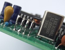
- The +12V converter module is mounted on the PCB on two small stacked, double-sided adhesive foam pads, and the bent-over pins connected to the board using some component wire offcuts, as shown in the close-up photo below.

Connecting to the Serial Port
A Terminal program running on a PC is required to communicate with the system. Configure the terminal for 19200 Baud, 7 data bits, even parity, 2 stop bits.
To connect the system to a 9-pin serial port on a PC, a serial cable with male and female connectors is required, with the following pins connected (as a minimum): 2‑2, 3‑3, 5‑5. If using a serial-USB adaptor,
you should be able to connect the serial adaptor to the system directly.
Versions of Cortex BASIC
Two versions of Cortex BASIC are included in the EPROM image:
- With the version of Cortex BASIC supplied with EVMBUG, the BASIC
interpreter code is
copied from EPROM to RAM and then run from RAM. This leaves 3K of memory
free for program storage, but this is often sufficient for 'tinkering', and
it is possible to tweak the BASIC interpreter itself if required as it is
resident in RAM. Set the EPROM bank select jumper J5 to the 'LO' position to select the lower 32K bank
to use this configuration.
- With the version of Cortex BASIC supplied with TIBUG, the BASIC
interpreter code
mostly runs direct from EPROM. This leaves 27K of memory free for program
storage. Set the EPROM bank select jumper J5 to the 'HI' position to select the
upper 32K bank to use this configuration. In addition, with this version:
- As BASIC programs are stored in the battery-backed RAM,
options are provided in the boot menu (described below) to select Cortex
BASIC and retain the current program in RAM (which can be subsequently
edited, listed or run), and to select Cortex BASIC and
automatically run the current program in RAM.
- The boot code checks the state of the TMS 9901 interface pin
connected to connector J4 pin 1 (the pin nearest the serial port connector)
and if it has been pulled low, the boot code automatically selects Cortex
BASIC and runs the current program in RAM. This gives the ability to
automatically run a BASIC program at power-on or system reset.
Boot Menu for EVMBUG System Monitor and Cortex BASIC
At power-on or reset, if J5 is set to the 'LO' position to select the lower
32K EPROM bank, EVMBUG waits for the user to press the "A" or <Return> key to
detect the terminal Baud rate, then the following boot menu is displayed:
TMS 9900 Project System
by Stuart Conner
Press 1 for
EVMBUG Monitor
Press 2 for Cortex BASIC
Press the number key indicated according to the option required.
Boot Menu for TIBUG System Monitor and Cortex BASIC
At power-on or reset, if J5 is set to the 'HI' position to select the upper
32K EPROM bank, the following boot menu is displayed (no requirement to press a
key to detect the Baud rate, which is fixed at 19200 Baud in TIBUG):
TMS 9900 Project System
by Stuart Conner
Press 1 for
TIBUG Monitor
Press 2 for Cortex BASIC (clear RAM)
Press 3 for Cortex
BASIC (retain current program in RAM)
Press 4 for Cortex BASIC (run current
program in RAM)
Note: options 3 and 4 will crash system if no BASIC
program currently loaded
Press the number key indicated according to the option required.
Programming - TIBUG and EVMBUG System Monitors
The TIBUG and EVMBUG system monitors provide an interactive interface between the user and the system.
They are described on this page.
If you are new to programming a single board computer of this type, the
user manual for the TM 990/100M microcomputer provides a good introduction to the processor architecture and concepts.
Programming - BASIC
The BASIC interpreter is based on a port of the
Powertran Cortex Power BASIC made for my
TM 990 computer. When
Cortex BASIC is selected from the boot menu, a message similar to the following
is displayed:
-- TMS 9900 Project BASIC Rev. 1.1 --
[Ported from Cortex BASIC (C)1982 by Stuart Conner]
*Ready
The Cortex BASIC user guide is available
here.
Mapping between the keys on the Cortex computer and the keys on the PC keyboard is as shown in the following table.
| Enter |
Return |
| Edit |
Ctrl-T |
| Clear |
Ctrl-L |
| Escape |
Esc |
| Graphic |
(not supported) |
| Insert |
Ctrl-V |
| Delete |
Ctrl-C |
| Rubout |
Backspace |
| Cursor Up |
Ctrl-E |
| Cursor Down |
Ctrl-X |
| Cursor Left |
Ctrl-S |
| Cursor Right |
Ctrl-D |
| Home |
Ctrl-H |
The version of EVMBUG/TIBUG supplied with BASIC is modified such that the automatic delay functionality after printing each line on a mechanical teletype is disabled. This won't make any difference unless you happen to be using a mechanical teletype ...
When BASIC is in use, all input is automatically converted to upper case.
There are some changes and restrictions in the TMS 9900 implementation as compared to the implementation described in the Cortex user guide:
- The following commands are not supported, and will display an error message if used: BOOT, MON, TIC, BAUD, MOTOR, TIME, LOAD, SAVE.
- The commands associated with text and graphics displays will be accepted and will execute, but as the system does not include a
video display processor, nothing will be seen.
- The UNIT command supports a value of 2 only (all input and output over the RS-232 interface).
- Pressing the <Space> key pauses a listing, then pressing any key resumes the listing. Stepping through the listing line-by-line is not currently supported.
- SYS values 10, 13-17, 19 are not relevant and will return -1.
- A new SYS value of 20 returns the address of the colour substitution table used by the SWAP command (see the addendum to the COLOUR command on page 4-77 of the user guide).
- The WAIT statement without an argument returns immediately. With an argument, no input is accepted and the <Escape> key is not active until the wait period expires. The wait period is significantly shorter than the 0.01 seconds quoted.
- There is a bug in the original implementation of the CHAR statement. When typing in a program, you need to put a space between the line number and the CHAR statement otherwise an 'Illegal Character' error is displayed.
- Memory addresses mentioned in the user guide and the memory maps are not correct for the TMS 9900 implementation. I can provide memory usage details if required.
Programming - Forth
The Forth interpreter is based on the fig-FORTH 9900 Release 1.0 (March 1981). The source code is available here (the TMS 9900 implementation is slightly modified in terms of the memory pointers used and the input/output routines). Forth is programmed in the EPROM along with a slightly modified version of the EVMBUG monitor. When the system is reset, a menu is displayed: press 1 to run the EVMBUG monitor, or press 2 to run Forth.
TMS 9900 Project System
by Stuart Conner
Press 1 for EVMBUG Monitor
Press 2 for fig-FORTH
(Press 2)
9900 fig-FORTH Rel 1.0
The Forth code is copied from EPROM to RAM and then run from RAM when it is selected at the menu. All input and output is over the RS-232 interface, and there is no means of loading or saving a program.
Various Forth tutorials are available here. Note that different versions of Forth support slightly different dictionaries so you might find some examples in the tutorials that will not work on the TMS 9900 implementation.
The version of EVMBUG supplied with Forth is modified such that the automatic delay functionality after printing each line on a mechanical teletype is disabled. This won't make any difference unless you happen to be using a mechanical teletype ...
Examples of Using the EVMBUG IC (Inspect/Change CRU) Command
This section provides examples of using the EVMBUG IC (Inspect/Change CRU)
command and how to interpret the command response. The examples are based around
the TMS 9901 programmable systems interface IC. When the 9901 is reset, all its
input/output pins are programmed as inputs, and their default logic state is
determined by the pull-up/down resistors networks RN1, RN2 and RN3 - see the circuit diagram.
The 9901 CRU base address is >40.
Entering the command IC 40 reads CRU
bits 0 - 15 from the 9901 and gives a response of >FFFE. To understand this
response, it is necessary to remember that the values in the response are
right-justified - that is, the first CRU bit read is the last bit in the
response - and to understand which 9901 pins are pulled high and which are
pulled low, as summarised in the table below which lists the CRU bits as defined
in the TMS 9901 data manual.
Reading the command response >FFFE backwards in binary, it is 0111 1111 1111 1111, and it can be seen that this matches the states of CRU bits 0
-
15 as shown in the table.
Entering the command IC 60 reads CRU
bits 16 - 31 from the 9901 and gives a response of >FF80. Reading this backwards
in binary it is 0000 0001 1111 1111, and it can be seen that this matches the
states of CRU bits 16 -
31 as shown in the table.
For an example of writing a CRU bit, connect a voltmeter, logic probe or oscilloscope to
J3 pin 7 (the pin nearest the end of the board) which is the 9901 signal P6,
which as an input is pulled low by RN1. Enter the command IC 6C,1
to read a single CRU bit and the response should be
>0000, then enter 1<Return> to write a
logic 1 to the CRU bit (which programs it as an output) and you should see this pin go high. Enter IC 6C,1
again and the response should now be >0001. Enter 0<Return>
to write a logic 0 to the CRU bit and it should go low
again.
| >40 |
0 |
Control Bit |
0 = Interrupt Mode (power-up default)
1 =
Clock Mode |
| >42 |
1 |
/INT1 |
Pulled high by RN3 |
| >44 |
2 |
/INT2 |
| >46 |
3 |
/INT3 |
| >48 |
4 |
/INT4 |
| >4A |
5 |
/INT5 |
| >4C |
6 |
/INT6 |
| >4E |
7 |
/INT7 |
| >50 |
8 |
/INT8 |
Pulled high by RN2 |
| >52 |
9 |
/INT9 |
| >54 |
10 |
/INT10 |
| >56 |
11 |
/INT11 |
| >58 |
12 |
/INT12 |
| >5A |
13 |
/INT13 |
| >5C |
14 |
/INT14 |
| >5E |
15 |
/INT15 |
| >60 |
16 |
P0 Input |
Pulled low by RN1 and J5 |
| >62 |
17 |
P1 Input |
Pulled low by RN1 |
| >64 |
18 |
P2 Input |
| >66 |
19 |
P3 Input |
| >68 |
20 |
P4 Input |
| >6A |
21 |
P5 Input |
| >6C |
22 |
P6 Input |
| >6E |
23 |
P7 Input |
As /INT15 - /INT8 - pulled high
by RN2 |
| >70 |
24 |
P8 Input |
| >72 |
25 |
P9 Input |
| >74 |
26 |
P10 Input |
| >76 |
27 |
P11 Input |
| >78 |
28 |
P12 Input |
| >7A |
29 |
P13 Input |
| >7C |
30 |
P14 Input |
| >7E |
31 |
P15 Input |
As /INT7 - pulled high by RN3 |
CRU Instruction Displacement Counts
The CRU instructions develop CRU-bit addresses from the CRU base address contained in register R12.
The multiple-bit CRU instructions Store Communications Register (STCR) and Load Communications Register (LDCR) perform bit transfers starting at the CRU base address in R12.
The single-bit CRU instructions Set Bit One (SBO), Set Bit Zero (SBZ) and Test Bit (TB) develop a CRU-bit address from the CRU base address in R12 plus twice the signed
displacement count specified in the instruction ('twice' due to the way that the signed displacement is left-shifted by one place internally). But R12 doesn't
have to contain the base address of the particular CRU device - you can set it to address a specific CRU bit. So the
following set of instructions with different values in R12 and different
displacements will actually operate on the same CRU bit:
LI R12,>0040
SBO 10
LI R12,>0054
SBO 0
LI R12,>0068
SBO -10
Sometimes you need to be inventive like this if using LDCR and STCR
instructions for multiple-bit CRU transfers to bits in the middle of the device's CRU address range,
and you also need to do single-bit CRU transfers to addresses above or below
this -
set R12 as needed for LDCR and STCR, and use SBO/SBZ with the CRU bit numbers
(displacements) set as needed (negative value, where necessary) to operate on the
single CRU
bits needed.
Project - TMS 9901 to IDE Interface
This is a little project to implement an IDE interface through a TMS 9901
programmable systems interface IC, with the software to read and write to the
IDE drive written in Cortex BASIC. At the moment there is no file system as
such, it only reads and writes directly to sectors on the drive, so it is
perhaps a solution looking for a problem - a pseudo-vintage data logger perhaps!
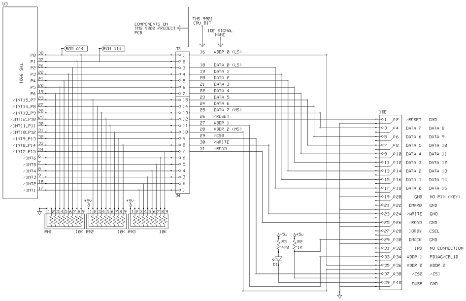
On the TMS 9900 PCB System, the programmable pins on the 9901 can be easily
accessed through the two header connectors. The circuit diagram is shown below.

On the PCB, some of the 9901 pins are connected to pull-up resistors and some
to pull-down resistors. When the 9901 is reset, all the pins are programmed as
inputs, so their default logic state is determined by the pull-up/down
resistors. When deciding how to connect the IDE interface, it is important that
the active low control signals /RESET, /CS0, /READ and /WRITE are connected to
pins on the 9901 that default to a high logic level such that the IDE drive
defaults to an 'inactive' state. The eight data lines are connected to pins
accessed through sequential CRU bits in the 9901 such that they can be set and
read using multi-bit CRU instructions.
The project is primarily focussed on Compact Flash IDE drives which can be
set to operate in an 8-bit mode - two 8-bit read/write operations take place for
each 16-bit data transfer. Although the hardware is also compatible with hard
drives, they do not support the 8-bit mode, which wastes half the data in each
512-byte sector. The 8-bit mode feature is selected on a Compact Flash drive by
writing >01 to the Feature register (register 1) then the >EF 'Set Feature'
command to the Command register (register 7).
As stated previously, when the 9901 is reset, all the pins are programmed as
inputs. Writing to a pin programs it as an output, and it remains as an output
until the 9901 is reset - either a hardware reset, or a software reset triggered
by writing to a specific CRU bit. Therefore when reading a sector from the
drive, the various registers on the drive are first programmed (by selecting a
register on the 3-bit address bus then writing a value on the data bus), then
the 9901 has to undergo a software reset such that the data bus pins can then be
used as inputs to read the data from the sector selected on the drive.
The software does not do any 'drive busy' checks on the drive before
performing operations. The couple of CF cards I have tried seem to have no
problems keeping up with an elderly 3 MHz processor running a BASIC interpreter!
Likewise there is no error detection - if it works it works, it if doesn't it
doesn't!
The Cortex BASIC software listing is shown below, along with an example
'session' writing data from memory to a sector and reading the data back again.
The program provides feedback on how the IDE drive registers are being
programmed for each operation.
100 REM TMS 9901 TO IDE INTERFACE
110 REM BY STUART CONNER, OCTOBER 2017
120 REM CORTEX BASIC
130 REM
140 REM **********************
150 REM *** INITIALISE CRU ***
160 REM **********************
170 BASE 040H+(2*18) !SET BASE ADDRESS TO CRU BIT 18 OF 9901
180 REM
190 REM ********************
200 REM *** DISPLAY MENU ***
210 REM ********************
220 PRINT "SELECT FROM THE FOLLOWING OPTIONS:"
230 PRINT "(1) WRITE A SECTOR WITH A SPECIFIED BYTE"
240 PRINT "(2) WRITE A SECTOR WITH DATA FROM MEMORY"
250 PRINT "(3) READ AND DISPLAY A SECTOR"
260 PRINT "(9) QUIT"
270 INPUT "OPTION",CH
280 IF CH=1 OR CH=2 THEN GOTO 360
290 IF CH=3 THEN GOTO 670
300 IF CH=9 THEN END
310 GOTO 270
320 REM
330 REM ********************
340 REM *** WRITE SECTOR ***
350 REM ********************
360 INPUT "SECTOR ADDRESS",SA
370 IF CH=1 THEN INPUT "BYTE TO WRITE",BYT
380 IF CH=2 THEN INPUT "MEMORY ADDRESS TO START WRITING FROM",ADS
390 GOSUB 1080 !RESET 9901
400 GOSUB 1000 !RESET IDE DRIVE
410 GOSUB 1470 !SET /CS0 LOW
420 GOSUB 1660 !SELECT MASTER DRIVE
430 GOSUB 1750 !SET 8-BIT MODE
440 NS=1: GOSUB 1870 !SET NUM OF SECTORS TO TRANSFER
450 GOSUB 1960 !SET SECTOR ADDRESS
460 REG=7: GOSUB 1160 !SELECT REGISTER 7 TO WRITE COMMAND
470 DAT=030H: GOSUB 1590 !SET DATA BUS FOR WRITE SECTOR COMMAND
480 GOSUB 1280 !PULSE /WRITE LOW
490 REG=0: GOSUB 1160 !SELECT REGISTER 0 TO WRITE DATA
500 PRINT "WRITING SECTOR:"
510 FOR I=1 TO 512/16
520 FOR J=1 TO 16
530 IF CH=1 THEN CRF[8]=BYT
540 IF CH=2 THEN CRF[8]=MEM[ADS]: ADS=ADS+1
550 GOSUB 1280 !PULSE /WRITE LOW
560 NEXT J
570 PRINT ".";
580 NEXT I
590 PRINT
600 GOSUB 1530 !SET /CS0 HIGH
610 PRINT
620 GOTO 220
630 REM
640 REM *******************
650 REM *** READ SECTOR ***
660 REM *******************
670 INPUT "SECTOR ADDRESS",SA
680 GOSUB 1080 !RESET 9901
690 GOSUB 1000 !RESET IDE DRIVE
700 GOSUB 1470 !SET /CS0 LOW
710 GOSUB 1660 !SELECT MASTER DRIVE
720 GOSUB 1750 !SET 8-BIT MODE
730 NS=1: GOSUB 1870 !SET NUM OF SECTORS TO TRANSFER
740 GOSUB 1960 !SET SECTOR ADDRESS
750 REG=7: GOSUB 1160 !SELECT REGISTER 7 TO WRITE COMMAND
760 DAT=020H: GOSUB 1590 !SET DATA BUS FOR READ SECTOR COMMAND
770 GOSUB 1280 !PULSE /WRITE LOW
780 GOSUB 1530 !SET /CS0 HIGH
790 GOSUB 1080 !RESET 9901 TO CHANGE DATA BUS TO INPUT
800 GOSUB 1470 !SET /CS0 LOW AGAIN
810 REG=0: GOSUB 1160 !SELECT REGISTER 0 TO READ DATA
820 PRINT "READING SECTOR (ALL VALUES IN HEX):"
830 FOR I=1 TO 512/16
840 FOR J=1 TO 16
850 GOSUB 1350 !SET /READ LOW
860 BYT=CRF[8]
870 GOSUB 1410 !SET /READ HIGH
880 PRINT #;BYT;" ";
890 NEXT J
900 PRINT
910 NEXT I
920 PRINT
930 GOSUB 1530 !SET /CS0 HIGH
940 PRINT
950 GOTO 220
960 REM
970 REM ***********************
980 REM *** RESET IDE DRIVE ***
990 REM ***********************
1000 PRINT "RESETTING IDE DRIVE"
1010 CRB[8]=0 !CRU BIT 26 (P0)
1020 CRB[8]=1
1030 RETURN
1040 REM
1050 REM ******************
1060 REM *** RESET 9901 ***
1070 REM ******************
1080 PRINT "RESETTING TMS 9901"
1090 CRB[-18]=1 !CRU BIT 0 (SET CLOCK MODE)
1100 CRB[-3]=0 !CRU BIT 15 (/RST2)
1110 RETURN
1120 REM
1130 REM ***********************************
1140 REM *** WRITE REGISTER NUMBER (0-7) ***
1150 REM ***********************************
1160 PRINT "ADDRESSING REGISTER";REG
1170 IF REG>=4 THEN CRB[10]=1: REG=REG-4 !CRU BIT 28 (P12)
1180 ELSE CRB[10]=0
1190 IF REG>=2 THEN CRB[9]=1: REG=REG-2 !CRU BIT 27 (P11)
1200 ELSE CRB[9]=0
1210 IF REG=1 THEN CRB[-2]=1 !CRU BIT 16 (P0)
1220 ELSE CRB[-2]=0
1230 RETURN
1240 REM
1250 REM ************************
1260 REM *** PULSE /WRITE LOW ***
1270 REM ************************
1280 CRB[12]=0 !CRU BIT 30 (P14)
1290 CRB[12]=1
1300 RETURN
1310 REM
1320 REM *********************
1330 REM *** SET /READ LOW ***
1340 REM *********************
1350 CRB[13]=0 !CRU BIT 31 (P15)
1360 RETURN
1370 REM
1380 REM **********************
1390 REM *** SET /READ HIGH ***
1400 REM **********************
1410 CRB[13]=1 !CRU BIT 31 (P15)
1420 RETURN
1430 REM
1440 REM ********************
1450 REM *** SET /CS0 LOW ***
1460 REM ********************
1470 CRB[11]=0 !CRU BIT 29 (P13)
1480 RETURN
1490 REM
1500 REM *********************
1510 REM *** SET /CS0 HIGH ***
1520 REM *********************
1530 CRB[11]=1 !CRU BIT 29 (P13)
1540 RETURN
1550 REM
1560 REM ********************
1570 REM *** SET DATA BUS ***
1580 REM ********************
1590 PRINT "SETTING DATA BUS TO";DAT;" (";#;DAT;"H)"
1600 CRF[8]=DAT
1610 RETURN
1620 REM
1630 REM ***************************
1640 REM *** SELECT MASTER DRIVE ***
1650 REM ***************************
1660 PRINT "SELECTING MASTER DRIVE (REG 6 AND DATA)"
1670 REG=6: GOSUB 1160 !SELECT REGISTER 6
1680 DAT=0E0H: GOSUB 1590 !SET DATA BUS
1690 GOSUB 1280 !PULSE /WRITE LOW
1700 RETURN
1710 REM
1720 REM **********************
1730 REM *** SET 8-BIT MODE ***
1740 REM **********************
1750 PRINT "SELECTING 8-BIT MODE (REG 1 AND DATA, REG 7 AND DATA)"
1760 REG=1: GOSUB 1160 !SELECT REGISTER 1 TO SET FEATURE
1770 DAT=01H: GOSUB 1590 !SET DATA BUS
1780 GOSUB 1280 !PULSE /WRITE LOW
1790 REG=7: GOSUB 1160 !SELECT REGISTER 7 TO WRITE COMMAND
1800 DAT=0EFH: GOSUB 1590 !SET DATA BUS
1810 GOSUB 1280 !PULSE /WRITE LOW
1820 RETURN
1830 REM
1840 REM *****************************************
1850 REM *** SET NUMBER OF SECTORS TO TRANSFER ***
1860 REM *****************************************
1870 PRINT "SETTING NUMBER OF SECTORS TO TRANSFER TO";NS;" (REG 2 AND DATA)"
1880 REG=2: GOSUB 1160 !WRITE NUM OF SECTORS TO TRANSFER TO REGISTER 2
1890 DAT=NS: GOSUB 1590 !SET DATA BUS
1900 GOSUB 1280 !PULSE /WRITE LOW
1910 RETURN
1920 REM
1930 REM *********************************************
1940 REM *** SET SECTOR (LBA) ADDRESS (0 TO 32767) ***
1950 REM *********************************************
1960 PRINT "SETTING SECTOR ADDRESS TO";SA;" (REG 3 AND DATA, REG 4 AND DATA, REG 5 AND DATA)"
1970 REG=3: GOSUB 1160 !WRITE SECTOR ADDRESS LBA 0 TO REGISTER 3
1980 DAT=SA LAND 0FFH: GOSUB 1590 !SET DATA BUS
1990 GOSUB 1280 !PULSE /WRITE LOW
2000 REG=4: GOSUB 1160 !WRITE SECTOR ADDRESS LBA 1 TO REGISTER 4
2010 DAT=SA/256 LAND 0FFH: GOSUB 1590 !SET DATA BUS
2020 GOSUB 1280 !PULSE /WRITE LOW
2030 REG=5: GOSUB 1160 !WRITE SECTOR ADDRESS LBA 2 TO REGISTER 5
2040 DAT=0H: GOSUB 1590 !SET DATA BUS
2050 GOSUB 1280 !PULSE /WRITE LOW
2060 RETURN
Example:
SELECT FROM THE FOLLOWING OPTIONS:
(1) WRITE A SECTOR WITH A SPECIFIED BYTE
(2) WRITE A SECTOR WITH DATA FROM MEMORY
(3) READ AND DISPLAY A SECTOR
(9) QUIT
OPTION? 2
SECTOR ADDRESS? 10
MEMORY ADDRESS TO START WRITING FROM? 0
RESETTING TMS 9901
RESETTING IDE DRIVE
SELECTING MASTER DRIVE (REG 6 AND DATA)
ADDRESSING REGISTER 6
SETTING DATA BUS TO 224 (E0H)
SELECTING 8-BIT MODE (REG 1 AND DATA, REG 7 AND DATA)
ADDRESSING REGISTER 1
SETTING DATA BUS TO 1 (01H)
ADDRESSING REGISTER 7
SETTING DATA BUS TO 239 (EFH)
SETTING NUMBER OF SECTORS TO TRANSFER TO 1 (REG 2 AND DATA)
ADDRESSING REGISTER 2
SETTING DATA BUS TO 1 (01H)
SETTING SECTOR ADDRESS TO 10 (REG 3 AND DATA, REG 4 AND DATA, REG 5 AND DATA)
ADDRESSING REGISTER 3
SETTING DATA BUS TO 10 (0AH)
ADDRESSING REGISTER 4
SETTING DATA BUS TO 0 (00H)
ADDRESSING REGISTER 5
SETTING DATA BUS TO 0 (00H)
ADDRESSING REGISTER 7
SETTING DATA BUS TO 48 (30H)
ADDRESSING REGISTER 0
WRITING SECTOR:
................................
SELECT FROM THE FOLLOWING OPTIONS:
(1) WRITE A SECTOR WITH A SPECIFIED BYTE
(2) WRITE A SECTOR WITH DATA FROM MEMORY
(3) READ AND DISPLAY A SECTOR
(9) QUIT
OPTION? 3
SECTOR ADDRESS? 10
RESETTING TMS 9901
RESETTING IDE DRIVE
SELECTING MASTER DRIVE (REG 6 AND DATA)
ADDRESSING REGISTER 6
SETTING DATA BUS TO 224 (E0H)
SELECTING 8-BIT MODE (REG 1 AND DATA, REG 7 AND DATA)
ADDRESSING REGISTER 1
SETTING DATA BUS TO 1 (01H)
ADDRESSING REGISTER 7
SETTING DATA BUS TO 239 (EFH)
SETTING NUMBER OF SECTORS TO TRANSFER TO 1 (REG 2 AND DATA)
ADDRESSING REGISTER 2
SETTING DATA BUS TO 1 (01H)
SETTING SECTOR ADDRESS TO 10 (REG 3 AND DATA, REG 4 AND DATA, REG 5 AND DATA)
ADDRESSING REGISTER 3
SETTING DATA BUS TO 10 (0AH)
ADDRESSING REGISTER 4
SETTING DATA BUS TO 0 (00H)
ADDRESSING REGISTER 5
SETTING DATA BUS TO 0 (00H)
ADDRESSING REGISTER 7
SETTING DATA BUS TO 32 (20H)
RESETTING TMS 9901
ADDRESSING REGISTER 0
READING SECTOR (ALL VALUES IN HEX):
FF B0 01 38 80 40 80 00 80 40 80 04 80 40 80 08
80 40 80 0C 80 60 80 10 80 60 80 14 80 60 80 18
80 60 80 1C 80 80 80 20 80 80 80 24 80 80 80 28
80 80 80 2C 80 A0 80 30 80 A0 80 34 80 A0 80 38
FF FF FF FF FF FF FF FF FF FF FF FF FF FF FF FF
FF FF FF FF FF FF FF FF FF FF FF FF FF FF FF FF
FF D4 05 C4 FF D4 05 62 FF D4 05 CE FF BA 04 F6
FF C6 01 BC FF C6 01 A0 FF D4 04 FC FF B0 06 10
02 E0 FF B0 04 C1 02 02 FF FC CC B1 02 01 05 FA
CC 81 02 09 00 80 02 0C 00 00 C8 0C FF DE 2F A0
01 E1 04 C0 04 C3 02 08 00 01 2E C5 2F A0 01 DA
06 A0 00 EA 42 01 06 04 43 03 06 2E 45 00 05 F8
46 07 08 9E 48 03 08 CE 4C 00 07 20 4D 03 05 04
4E 03 08 E8 4F 00 09 96 52 00 06 E8 57 01 06 7A
3F 00 08 E2 00 00 02 2B 00 03 C2 9B 13 1F 91 7B
16 FA D1 BB C2 DB 09 86 02 07 FF B0 09 16 17 0D
2E 44 01 12 01 26 CD C4 05 83 02 85 0D 00 13 05
10 F5 05 C7 02 85 0D 00 16 F7 04 5B 04 C0 10 08
02 00 00 01 10 05 02 00 00 02 10 02 02 00 00 04
2F A0 01 CE 2E 00 10 A4 02 0C FF F4 04 FC 07 3C
04 FC 04 DC 02 0C 00 00 C8 0C FF DE 1D 1F 32 20
02 5F 1E 0D 04 C3 02 07 01 7C 10 0B 1F 0F 13 FE
05 83 1F 0F 16 FD 02 07 01 7A 8D C3 12 02 05 C7
10 FC 33 17 04 60 0A 50 10 83 00 07 00 1A 00 0E
00 34 00 1D 00 68 00 3B 00 D0 00 75 01 A0 00 EA
03 40 02 46 04 D0 7F FF 06 38 61 00 7A 00 E0 00
1F 15 16 FE 04 DB 36 1B 1E 12 88 1B 01 9A 1A 05
88 1B 01 9C 1B 02 A6 E0 01 9E 03 80 1D 10 1F 16
16 FE 32 1B 1F 16 16 FE 1F 17 16 FC 03 80 0D 0A
45 52 52 4F 52 20 00 20 20 20 20 00 0D 0A 42 50
00 0D 0A 3F 3E 00 0D 0A 54 49 42 55 47 20 52 45
56 2E 42 20 28 63 6F 6D 6D 73 20 31 39 32 30 30
SELECT FROM THE FOLLOWING OPTIONS:
(1) WRITE A SECTOR WITH A SPECIFIED BYTE
(2) WRITE A SECTOR WITH DATA FROM MEMORY
(3) READ AND DISPLAY A SECTOR
(9) QUIT
OPTION?
Project - SBP 9900/9989
Processor Adaptor Board
The SBP 9900 microprocessor (datasheet)
is a ruggedised version of the TMS 9900 processor fabricated with Integrated
Injection Logic (I2L) technology. It is
intended for applications requiring efficient, stable, reliable performance in
severe operating environments. It operates from a single DC power source with
user-selectable speed/power performance. The SBP 9989 (datasheet)
is a second-generation version of the processor and offers twice the performance
of the original SBP 9900A.
The pinout of the SBP 9900/9989 is largely the same as the TMS 9900 with
exception of the power pins, clock, and a couple of new signals on pins which
were not used on the TMS 9900. Output pins require a 1.2K pullup resistor to
+5V.
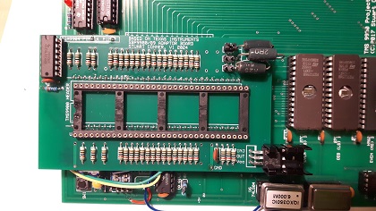
The adaptor board shown below (circuit diagram
here) enables an
SBP 9900 or 9989 to be plugged into a TMS 9900 socket. The board is
based on one produced by Texas Instruments. The board includes
options for three different injector current settings, has an on-board current regulator, and generates a suitable
clock from two wired connections to the TIM 9904 clock generator IC. Early versions
of the SBP 9900 have a maximum clock frequency of 2 MHz so use of the adaptor
board may require the TIM 9904 crystal and timing components to be changed to
generate a slower clock (the Baud rate of the TMS 9902 will be reduced in
proportion which will require a slower Baud rate to be selected in the Terminal
program).

The board has two rows of 32 header pins on the bottom which plug into the
original TMS 9900 socket.
These header pins were found suitable to plug into a turned pin socket.

 Description
 Specification
 Parts List
 Technical Description
 References
 EPROM Binary Images
 Assembling the PCB
 Connecting to the Serial Port
 Versions of Cortex BASIC
 Programming - TIBUG and EVMBUG System Monitors
 Programming - BASIC
 Programming - Forth
 Examples of Using the EVMBUG IC (Inspect/Change CRU) Command
 CRU Instruction Displacement Counts
 Project - TMS 9901 to IDE Interface
 Project - SBP 9900/9989
Processor Adaptor Board